
The Definitive Guide to Quantum Dots: Nanoscale Semiconductors Revolutionizing Green Energy and Technology
- Green Fuel Journal

- Dec 24, 2025
- 22 min read
Introduction & Fundamentals of Quantum Dots
What Are Quantum Dots? A Simple Definition
Quantum Dots are nanoscale semiconductor crystals, typically measuring between 2 to 10 nanometers in diameter—roughly 50,000 times smaller than the width of a human hair. Quantum Dots exhibit unique optical and electronic properties due to quantum confinement effects, allowing them to emit precise colors of light when energized. These semiconductor nanocrystals have emerged as transformative materials in renewable energy applications, display technologies, biomedical imaging, and quantum computing.
The Green Fuel Journal Research Team has identified Quantum Dots as critical components in next-generation solar cells, photocatalytic hydrogen production systems, and energy-efficient lighting technologies. Their ability to be tuned to absorb and emit specific wavelengths of light makes Quantum Dots invaluable for capturing broader spectrums of solar energy and improving the efficiency of renewable energy systems.
The Quantum Confinement Effect: Why Size Matters at the Nanoscale
The remarkable properties of Quantum Dots stem from a phenomenon called quantum confinement. When semiconductor materials are reduced to dimensions smaller than the exciton Bohr radius—typically around 10 nanometers or less—electrons and holes (positive charges) become spatially confined. This confinement fundamentally changes how these particles behave compared to bulk semiconductor materials.
In bulk semiconductors like silicon or cadmium selenide, electrons can move freely throughout the material's crystal lattice. The bandgap—the energy difference between the valence band (where electrons normally reside) and the conduction band (where electrons can move freely to conduct electricity)—remains fixed regardless of the material's size.
However, when you shrink a semiconductor down to quantum dot dimensions, something fascinating happens. The electrons and holes can no longer move freely in all directions. They become confined to a tiny three-dimensional space, similar to how a ball bouncing in a small box has limited movement compared to one bouncing in a large room.
This spatial confinement creates discrete energy levels rather than continuous energy bands. Think of it like a musical instrument: a long guitar string can vibrate at many different frequencies, producing a range of tones. But if you shorten that string significantly, it can only vibrate at specific, distinct frequencies. Similarly, confined electrons in Quantum Dots can only exist at specific energy levels.
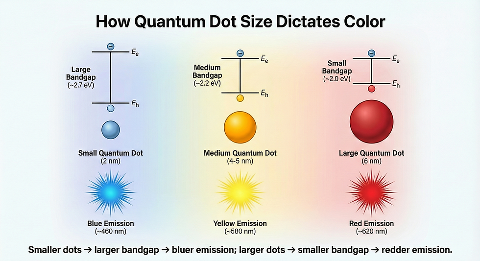
The practical result: Smaller Quantum Dots have larger bandgaps and emit higher-energy (bluer) light, while larger Quantum Dots have smaller bandgaps and emit lower-energy (redder) light. A 2-nanometer cadmium selenide Quantum Dot might glow blue, while a 6-nanometer dot of the same material glows red. This size-tunable emission is the foundation of Quantum Dot applications in displays, solar cells, and lighting.
The Brus Equation: Calculating Quantum Confinement
The relationship between Quantum Dot size and bandgap energy was mathematically described by Professor Louis E. Brus at Bell Laboratories in 1984. The Brus Equation allows scientists to predict the optical properties of Quantum Dots based on their size.
The simplified Brus Equation looks like this:
E(QD) = E(bulk) + (h²/8R²) × (1/m_e + 1/m_h) - 1.8e²/εR
Let's break this down into understandable components:
E(QD) = The bandgap energy of the Quantum Dot
E(bulk) = The bandgap energy of the bulk semiconductor material
h = Planck's constant (6.626 × 10⁻³⁴ joule-seconds)
R = The radius of the Quantum Dot
m_e = The effective mass of the electron
m_h = The effective mass of the hole (positive charge)
e = The elementary charge (1.602 × 10⁻¹⁹ coulombs)
ε = The dielectric constant of the semiconductor material
What does this mean in practical terms?
The equation tells us that the Quantum Dot's energy increases as its radius (R) decreases. The (h²/8R²) term shows an inverse square relationship—if you halve the size of a Quantum Dot, its confinement energy increases by a factor of four. This is why tiny changes in Quantum Dot size during synthesis can produce dramatically different colors.
The second term, -1.8e²/εR, represents the Coulombic attraction between the electron and hole. As the dot gets smaller, this attractive force also increases, but it has a smaller effect than the confinement energy.
Real-world example:
For cadmium selenide (CdSe) Quantum Dots, the bulk bandgap is approximately 1.74 electron volts (eV), corresponding to red light. A 2-nm CdSe Quantum Dot has a bandgap of around 2.7 eV (blue light), while a 6-nm dot has a bandgap of approximately 2.0 eV (orange-red light).
This 1 eV difference from just 4 nanometers of size change demonstrates the power of quantum confinement.
Types of Quantum Dots: Material Categories and Structures
Quantum Dots are not a single material but rather a diverse family of nanostructures. The Green Fuel Journal Research Team categorizes them based on composition and structural design:
1. Traditional Semiconductor Quantum Dots
Cadmium-Based Quantum Dots (CdSe, CdS, CdTe)
Cadmium selenide (CdSe) has been the workhorse material for Quantum Dot research since the 1980s. These dots offer exceptional quantum yields (often exceeding 85%), narrow emission spectra (25-30 nanometer full-width half maximum), and well-understood synthesis protocols.
Key characteristics:
Emission range: 470-650 nanometers (blue to red)
Quantum yield: 70-95% depending on surface treatment
Synthesis temperature: 150-320°C for colloidal methods
Primary applications: Display technologies, biomedical imaging
Environmental concern: Cadmium is a heavy metal listed under the EU's Restriction of Hazardous Substances (RoHS) directive. The European Union limits cadmium content to 0.01% by weight in electronic equipment, creating regulatory challenges for commercial Quantum Dot products.
Indium Phosphide (InP) Quantum Dots
In response to cadmium toxicity concerns, indium phosphide has emerged as the leading cadmium-free alternative. Samsung and TCL have commercialized InP-based QLED televisions since 2019, demonstrating the viability of non-toxic Quantum Dots.
Key characteristics:
Emission range: 500-700 nanometers (green to red)
Quantum yield: 60-85% (improving with core-shell engineering)
Synthesis challenges: More sensitive to oxidation than CdSe
Cost factor: Indium is approximately 3-5 times more expensive than cadmium by weight
Lead Halide Perovskite Quantum Dots
Perovskite Quantum Dots (general formula CsPbX₃, where X = Cl, Br, I) represent the newest class of semiconductor nanocrystals, first reported by Professor Loredana Protesescu at ETH Zurich in 2015.
Key characteristics:
Emission range: 410-700 nanometers (violet to deep red)
Quantum yield: 50-90% depending on composition
Synthesis advantage: Room-temperature synthesis possible
Stability challenge: Highly sensitive to moisture and oxygen
Solar cell efficiency: 16.6% certified efficiency in perovskite Quantum Dot solar cells as of 2024
Sustainability perspective: While perovskites contain lead (another toxic heavy metal), the amount used in thin-film applications is significantly less than in lead-acid batteries. Research groups at Stanford University and University of Oxford are developing lead-free alternatives using tin (Sn) and bismuth (Bi).
2. Carbon-Based Quantum Dots (The Green Alternative)
Carbon Quantum Dots (CQDs) and Graphene Quantum Dots (GQDs) represent the most environmentally friendly class of Quantum Dots. These carbon-based nanostructures are composed entirely of carbon, hydrogen, and oxygen—elements abundant in nature and non-toxic to biological systems.
Carbon Quantum Dots (CQDs)
CQDs are quasi-spherical nanoparticles, typically 2-10 nanometers in diameter, composed of sp² and sp³ hybridized carbon atoms. Unlike semiconductor Quantum Dots, CQDs emit light primarily due to surface states and functional groups rather than pure quantum confinement.
Key characteristics:
Emission range: 400-650 nanometers (tunable by surface modification)
Quantum yield: 10-80% (highly dependent on synthesis method)
Biocompatibility: Excellent—demonstrated in in vivo imaging studies
Synthesis sources: Can be produced from biomass waste, citric acid, glucose, or even orange peel
Green synthesis breakthrough: In 2023, researchers at the Indian Institute of Technology (IIT) Bombay successfully synthesized CQDs from sugarcane bagasse—a waste product from sugar production. This process converts agricultural waste into valuable nanomaterials, aligning perfectly with circular economy principles.
Graphene Quantum Dots (GQDs)
GQDs are single or few-layer graphene sheets with lateral dimensions below 20 nanometers. They combine the exceptional electrical conductivity of graphene with quantum confinement effects.
Key characteristics:
Thickness: Typically 1-3 graphene layers (0.34-1.0 nanometers)
Lateral size: 5-20 nanometers
Edge effects: Zigzag vs. armchair edges produce different electronic properties
Applications: Supercapacitors, photocatalysis, transparent conductors
Environmental advantage: GQDs can be synthesized from graphite waste or coal using electrochemical exfoliation, potentially transforming carbon-intensive materials into high-value green technology components.
3. Core-Shell Quantum Dot Architectures
To enhance quantum yield, photostability, and chemical resistance, researchers engineer core-shell Quantum Dots—nanostructures where a protective shell material surrounds the emissive core.
Common Core-Shell Designs:
Structure | Core Material | Shell Material | Quantum Yield | Primary Benefit |
Type I | CdSe | ZnS | 85-95% | Passivates surface defects, prevents oxidation |
Type II | CdTe | CdSe | 60-75% | Extends emission to near-infrared |
Graded | CdSe | CdS (gradual) | 80-90% | Reduces lattice strain, improves stability |
Multi-shell | InP | ZnSe/ZnS | 70-85% | Compensates for lower InP quantum yield |
How core-shell design works:
The shell material has a wider bandgap than the core. When an electron-hole pair is created in the core and tries to move to the surface, it encounters an energy barrier created by the shell. This barrier confines the charge carriers within the core, preventing them from reaching surface defects where they would lose energy as heat instead of light.
Example:
A CdSe/ZnS core-shell Quantum Dot might have a 4-nanometer CdSe core surrounded by a 2-monolayer ZnS shell (approximately 0.6 nanometers thick).
This shell increases the quantum yield from 30-40% (bare CdSe) to 85-95% (core-shell structure).
Sustainability consideration: Core-shell designs allow the use of less toxic materials in the shell while retaining high-performance cores.
For instance, CdSe/ZnS dots require 60-70% less cadmium by mass compared to bare CdSe dots of equivalent brightness, reducing environmental impact while maintaining performance.
Synthesis & Manufacturing of Quantum Dots
Top-Down vs. Bottom-Up Approaches: Two Pathways to Nanoscale Precision

Quantum Dot synthesis follows two fundamental manufacturing philosophies that differ in their starting points and fabrication mechanisms.
Top-Down Approaches: Breaking Down Bulk Materials
Top-down synthesis begins with bulk semiconductor materials and uses physical or chemical processes to reduce them to nanoscale dimensions. This approach mirrors traditional semiconductor manufacturing techniques used in microelectronics.
Primary top-down methods:
Electron-beam lithography: Uses focused electron beams to pattern Quantum Dots on semiconductor wafers. This method achieves excellent spatial control, positioning dots with sub-5-nanometer precision. However, it's extremely slow (1-2 hours per square centimeter) and economically viable only for specialized applications like quantum computing research.
Ion implantation: Bombards semiconductor substrates with high-energy ions to create localized defect regions that can be converted into Quantum Dots. Research teams at IBM and Intel have explored this method for integrating Quantum Dots into existing silicon chip manufacturing.
Laser ablation: Focuses high-power laser pulses onto semiconductor targets in liquid media. The intense energy vaporizes material, which then condenses into nanoparticles. Pulsed laser ablation can produce 2-8 nanometer Quantum Dots but struggles with size uniformity—typical batches show ±30% size variation.
Limitations of top-down approaches:
High energy consumption: Often requires vacuum chambers and high-temperature processing (>500°C)
Material waste: 70-85% of starting material is removed and cannot be recovered
Limited scalability: Production rates typically under 1 gram per day
Cost: Equipment costs range from $500,000 to $2 million for research-grade systems
Bottom-Up Approaches: Building Atoms into Quantum Dots
Bottom-up synthesis assembles Quantum Dots atom-by-atom or molecule-by-molecule from chemical precursors. This approach dominates commercial Quantum Dot production due to superior scalability and cost-effectiveness.
Advantages of bottom-up methods:
High throughput: Industrial reactors produce kilograms per batch
Better size control: Achieves ±5-10% size distribution
Lower cost: Precursor materials cost $50-200 per kilogram compared to wafer-based methods
Room for green chemistry: Compatible with bio-based precursors and aqueous synthesis
Colloidal Synthesis: The Gold Standard for Quantum Dot Production
Colloidal synthesis, also called hot-injection synthesis, has become the dominant method for producing high-quality Quantum Dots since its development by Dr. Christopher Murray and Dr. Moungi Bawendi at MIT in 1993. This technique won recognition as one of the top chemical discoveries of the 20th century.
The Hot-Injection Process: Step-by-Step
Step 1: Precursor Preparation
Chemical precursors containing the semiconductor elements are dissolved in high-boiling-point organic solvents. For CdSe Quantum Dots:
Cadmium precursor: Cadmium oxide (CdO) or cadmium acetate dissolved in oleic acid
Selenium precursor: Selenium powder dissolved in trioctylphosphine (TOP) or octadecene
Coordinating solvents: Oleylamine, oleic acid, or trioctylphosphine oxide (TOPO)
Step 2: High-Temperature Nucleation
The cadmium solution is heated to 280-320°C under inert atmosphere (nitrogen or argon). At this temperature, the selenium precursor is rapidly injected into the hot cadmium solution. This sudden injection creates supersaturation—the solution contains more dissolved material than it can normally hold at that temperature.
Critical timing: The injection takes 1-3 seconds. Too slow, and you get continuous nucleation with poor size control. Too fast, and you risk temperature drops that affect crystal quality.
Step 3: Nucleation Burst
The supersaturation triggers a rapid nucleation event where thousands of CdSe nuclei (tiny crystal seeds 1-2 nanometers in size) form simultaneously. This burst lasts only 2-5 seconds but determines the final Quantum Dot population.
The "LaMer model" explains this process: nucleation occurs only when supersaturation exceeds a critical threshold. Once nucleation begins, it rapidly depletes the supersaturation, preventing new nuclei from forming. This self-limiting process is key to producing uniform Quantum Dots.
Step 4: Controlled Growth
After nucleation, the temperature is reduced to 250-280°C for the growth phase. Remaining precursors in solution deposit onto existing nuclei, growing them into larger Quantum Dots. Growth follows Ostwald ripening—larger particles grow at the expense of smaller ones, gradually narrowing the size distribution.
Growth kinetics:
First 30 seconds: Rapid growth (0.1-0.2 nm/second)
1-10 minutes: Slower growth (0.01-0.05 nm/second)
After 10 minutes: Minimal growth, size refinement through ripening
Size control: Sampling the reaction at different times produces different-sized Quantum Dots:
30 seconds: 2-3 nm (blue emission, ~460 nm)
2 minutes: 3-4 nm (green emission, ~520 nm)
5 minutes: 4-5 nm (yellow emission, ~580 nm)
10 minutes: 5-6 nm (red emission, ~620 nm)
Step 5: Purification and Surface Passivation
After growth, the Quantum Dots are cooled and washed with polar solvents (methanol, acetone, or ethanol) to remove excess precursors and byproducts. The dots precipitate and are redispersed in non-polar solvents (hexane, toluene, or chloroform) for storage.
Surface ligands (oleic acid, oleylamine) remain attached to the Quantum Dot surface, providing colloidal stability and preventing aggregation. These organic molecules are crucial—without them, Quantum Dots clump together within minutes and lose their optical properties.
Material-Specific Synthesis Protocols
Cadmium Selenide (CdSe): The Reference Standard
CdSe synthesis is the most mature and reproducible Quantum Dot manufacturing process. Industrial producers like Nanosys (acquired by Shoei Chemical in 2022) and Nanoco manufacture multi-kilogram batches with quantum yields exceeding 90%.
Optimized CdSe recipe (research scale):
Cadmium precursor: 0.4 mmol CdO + 4 mL oleic acid
Selenium precursor: 0.2 mmol Se + 2 mL trioctylphosphine
Solvent: 20 mL octadecene
Nucleation temperature: 310°C
Growth temperature: 270°C
Reaction time: 3-8 minutes depending on target size
Yield: ~150 mg of Quantum Dots per batch
Indium Phosphide (InP): Overcoming Synthesis Challenges
InP Quantum Dots present significantly greater synthesis challenges than CdSe due to the high reactivity of phosphorus precursors and sensitivity to oxidation.
Major challenges:
Precursor reactivity: Tris(trimethylsilyl)phosphine ((TMS)₃P), the most common phosphorus source, reacts violently with air and moisture
Multiple oxidation states: Indium exists in In⁺ and In³⁺ states; controlling which state dominates affects crystal quality
Surface oxidation: InP oxidizes to InPO₄ within hours of air exposure, degrading optical properties
Lower quantum yield: Bare InP cores typically show 10-30% quantum yield compared to 40-60% for bare CdSe
InP synthesis breakthrough (2015-2018):
Researchers at University of Rochester and Samsung Advanced Institute of Technology independently developed zinc carboxylate protocols that dramatically improved InP quality.
Adding zinc stearate during synthesis:
Reduces surface oxidation by 75%
Increases quantum yield to 60-70% (without shell)
Improves size distribution to ±8-10%
Modern InP/ZnSeS/ZnS core-shell protocol:
Indium precursor: Indium acetate + oleic acid
Phosphorus precursor: (TMS)₃P in octadecene
Zinc precursor: Zinc stearate (added during synthesis)
Shell materials: ZnSe (inner shell) + ZnS (outer shell)
Final quantum yield: 75-85%
Production cost: $800-1,200 per kilogram (bulk industrial scale)
Why InP matters for green energy: Samsung's QD-OLED televisions using InP Quantum Dots consume 30-40% less power than conventional LCD displays of equivalent brightness, translating to significant energy savings across millions of units sold globally.
Hydrothermal Synthesis: Water-Based Green Chemistry
Hydrothermal synthesis produces Quantum Dots in aqueous solutions at temperatures between 120-250°C under elevated pressure (10-50 bar). This method has gained attention for manufacturing carbon-based Quantum Dots and certain metal oxide Quantum Dots using environmentally benign solvents.
Process overview:
Step 1: Precursors are dissolved in water along with stabilizing agents (citric acid, polyvinylpyrrolidone, or amino acids)
Step 2: The solution is sealed in a stainless steel autoclave (a high-pressure reactor)
Step 3: The autoclave is heated to 150-220°C, creating autogenous pressure (10-30 bar) from water vapor
Step 4: Quantum Dots nucleate and grow over 4-24 hours
Step 5: After cooling, Quantum Dots are recovered by centrifugation or dialysis
Advantages for carbon Quantum Dots:
Non-toxic solvents: Pure water eliminates hazardous organic solvents
Biomass compatibility: Can use glucose, citric acid, amino acids, or even food waste as carbon sources
Functionalized surfaces: Water-soluble Quantum Dots emerge with hydroxyl (-OH) and carboxyl (-COOH) groups ideal for biomedical applications
Scalability: Industrial autoclaves handle 100-1,000 liter batches
Case study - Green synthesis from agricultural waste:
In 2024, researchers at Tamil Nadu Agricultural University synthesized carbon Quantum Dots from rice husk ash using hydrothermal treatment. The process:
Converted 10 tons of rice husk waste (an agricultural burden) into 500 kg of carbon Quantum Dots
Achieved 45% quantum yield suitable for LED applications
Production cost: $15-20 per kilogram (compared to $200-500/kg for conventional carbon Quantum Dots)
Carbon footprint: 85% lower than organic solvent-based synthesis
This demonstrates how Quantum Dot manufacturing can integrate into circular economy frameworks, transforming waste streams into valuable green technology materials.
Laser Ablation: Precision Manufacturing for Specialty Applications
Pulsed laser ablation in liquid (PLAL) uses high-intensity laser pulses to vaporize solid targets immersed in liquids, creating Quantum Dots through rapid quenching of the vapor plume.
Process mechanics:
A nanosecond or picosecond pulsed laser (typically Nd:YAG at 1064 nm or 532 nm) focuses onto a semiconductor target submerged in water or organic solvent. Each laser pulse:
Deposits gigawatts per square centimeter of power in nanoseconds
Creates a localized plasma with temperatures exceeding 10,000 K
Vaporizes a microscopic amount of target material
Forms a cavitation bubble that collapses within microseconds
Rapidly quenches vaporized material into nanoparticles
Typical parameters:
Laser wavelength: 532 nm or 1064 nm
Pulse duration: 5-10 nanoseconds
Pulse energy: 50-200 millijoules
Repetition rate: 10-100 Hz
Ablation time: 10-60 minutes
Production rate: 0.1-1 gram per hour
Advantages:
Ultra-pure Quantum Dots: No chemical precursors means no contamination
Ligand-free surfaces: Ideal for catalysis applications where organic ligands interfere
Alloy capability: Can ablate multi-element targets to create alloyed Quantum Dots
Limitations:
Low throughput: 100-1,000 times slower than colloidal synthesis
Broad size distribution: Typical ±25-40% size variation
High energy consumption: 5-10 kWh per gram of Quantum Dots
Equipment cost: Pulsed lasers cost $30,000-150,000
Niche applications: Laser ablation excels for creating ligand-free carbon Quantum Dots for photocatalysis and alloyed Quantum Dots (like CdSeS or InPZnS) difficult to synthesize chemically.
Green Synthesis: Aligning Quantum Dot Production with Sustainability
Plant Extract-Based Synthesis
Phytochemicals (natural compounds in plants) can reduce metal ions and stabilize Quantum Dots without toxic chemicals. Plants produce polyphenols, flavonoids, terpenoids, and alkaloids that act as both reducing agents and capping ligands.
Documented green synthesis examples:
Plant Source | Quantum Dot Type | Size Range | Quantum Yield | Research Institution | Year |
Aloe vera extract | CdS | 3-5 nm | 35-45% | University of Pune, India | 2018 |
Tea leaf extract | ZnO | 4-8 nm | 28-38% | IIT Kharagpur, India | 2019 |
Lemon peel extract | Carbon QDs | 2-4 nm | 52-61% | University of Hyderabad, India | 2021 |
Neem leaf extract | Ag₂S | 5-10 nm | 18-25% | Anna University, India | 2020 |
Banana peel | N-doped Carbon QDs | 3-6 nm | 48-56% | IIT Bombay, India | 2023 |
The neem leaf synthesis process (simplified):
Step 1: 50 grams of fresh neem leaves are washed and boiled in 500 mL distilled water for 30 minutes
Step 2: The extract is filtered and cooled to room temperature
Step 3: Silver nitrate (AgNO₃) and sodium sulfide (Na₂S) solutions are added dropwise to 100 mL of extract
Step 4: The mixture is stirred at 60°C for 2-4 hours until color change indicates Quantum Dot formation
Step 5: Quantum Dots are collected by centrifugation and washed with ethanol
Results: 2-4 nm Ag₂S Quantum Dots with near-infrared emission (~820 nm) suitable for bioimaging applications
Environmental benefits:
Zero toxic solvents: Pure water-based process
Renewable resources: Plant materials are sustainable and widely available
Low energy: Room temperature to 60°C processing (compared to 280-320°C for traditional synthesis)
Waste valorization: Can utilize agricultural waste (peels, leaves, husks)
Current limitations:
Lower quantum yields: Typically 20-60% vs 80-95% for optimized chemical synthesis
Batch-to-batch variation: Plant extract composition varies by season, soil, and growing conditions
Scaling challenges: Industrial-scale plant extract sourcing and standardization remain undeveloped
Industrial Scaling: From Lab Bench to Manufacturing Floor
Transitioning Quantum Dot production from milligram research batches to multi-kilogram industrial output presents formidable engineering challenges.
The scaling problem:
A typical research synthesis produces 100-500 mg of Quantum Dots in a 50-100 mL flask. A QLED television factory requires 5-10 kilograms per day to coat display panels. This represents a 10,000-20,000× scale-up.
Key scaling challenges:
1. Heat Management
The hot-injection synthesis releases substantial heat during nucleation. In a small flask, this heat dissipates quickly. In a 100-liter reactor, poor heat removal creates temperature gradients that produce non-uniform Quantum Dots.
Solution: Industrial reactors use jacketed vessels with recirculating heat transfer fluids maintaining ±2°C temperature uniformity. Computational fluid dynamics (CFD) modeling optimizes stirring patterns to eliminate hot spots.
2. Mixing Uniformity
Rapid precursor injection must achieve <1 second mixing time across the entire reactor volume to replicate the sudden supersaturation crucial for monodisperse nucleation.
Solution: High-shear mixers operating at 1,000-3,000 RPM and multi-point injection systems that simultaneously inject precursor at 4-8 locations around the reactor.
3. Oxygen and Moisture Contamination
Parts-per-million levels of oxygen oxidize precursors and growing Quantum Dots, degrading quality. Maintaining inert atmosphere in 100+ liter vessels is complex.
Solution: Continuous nitrogen purging, oxygen sensors with <0.1 ppm detection limits, and glovebox-integrated reactors for highly sensitive materials like InP.
4. Reproducibility and Quality Control
Consumer electronics require ±3% variation in emission wavelength across production batches. Achieving this demands rigorous process control.
Industrial quality control protocol:
In-line UV-Vis spectroscopy: Monitors absorption during synthesis
Photoluminescence measurement: Real-time quantum yield tracking
Dynamic light scattering (DLS): Confirms size distribution
Transmission electron microscopy (TEM): Spot-checks size and crystallinity
Inductively coupled plasma mass spectrometry (ICP-MS): Verifies elemental composition
Production economics at scale:
Scale | Batch Size | Production Rate | Cost per kg | Quantum Yield | Application |
Research lab | 0.1-0.5 g | 1-5 g/month | $10,000-50,000 | 85-95% | Proof of concept |
Pilot plant | 10-50 g | 0.5-2 kg/month | $2,000-5,000 | 80-90% | Product development |
Industrial | 5-20 kg | 100-500 kg/month | $200-800 | 75-85% | Commercial production |
Mega-scale | 50-100 kg | 1,000+ kg/month | $50-200 | 70-80% | Mass market displays |
Case study - Nanosys industrial production:
Nanosys, the leading Quantum Dot manufacturer before its 2022 acquisition, achieved:
Batch sizes: 20-30 kg of core-shell Quantum Dots
Production capacity: 200+ tons annually at peak
Quality: ±2 nm emission wavelength consistency
Cost: Estimated $300-600 per kg for display-grade material
Customers: Samsung, TCL, Hisense for QLED televisions
This scale enabled over 30 million QLED TVs shipped globally by 2023, demonstrating successful transition from laboratory curiosity to mainstream consumer technology.
Properties, Stability, and Environmental Impact
Photoluminescence: The Light-Emitting Magic of Quantum Dots
Photoluminescence is the process by which Quantum Dots absorb high-energy photons (ultraviolet or blue light) and re-emit lower-energy photons (visible light) in specific colors. This property makes Quantum Dots invaluable for displays, lighting, and solar energy harvesting.
The photoluminescence mechanism:
Step 1: Photon Absorption
When a photon with energy greater than the Quantum Dot's bandgap strikes the nanocrystal, an electron in the valence band absorbs the energy and jumps to the conduction band. This leaves behind a positively charged "hole" in the valence band. The electron-hole pair is called an exciton.
Step 2: Thermalization
The excited electron quickly loses excess energy through phonon emission (lattice vibrations) and relaxes to the bottom of the conduction band. This process takes 100-500 femtoseconds (10⁻¹³ seconds).
Step 3: Radiative Recombination
The electron and hole recombine, releasing energy as a photon. The photon's energy (and thus its color) corresponds precisely to the bandgap energy of the Quantum Dot. This process typically occurs within 10-100 nanoseconds.
Example: A 4.5 nm CdSe Quantum Dot has a bandgap of ~2.2 eV, corresponding to 564 nm (green light). When illuminated with UV light (365 nm, 3.4 eV), it absorbs the high-energy photons and emits pure green light.
Emission spectrum characteristics:
Quantum Dots produce remarkably narrow emission spectra—typically 25-35 nm full-width half-maximum (FWHM).
In comparison:
Organic dyes: 50-80 nm FWHM
Phosphors: 60-100 nm FWHM
White LEDs: 100+ nm FWHM
This narrow emission creates saturated, pure colors ideal for display technologies. Samsung's QLED televisions achieve 100% of the DCI-P3 color space and >90% of Rec. 2020 thanks to Quantum Dot color purity.
Quantum Yield: Measuring Light-Emitting Efficiency
Quantum yield (QY) measures the efficiency of photoluminescence—the ratio of photons emitted to photons absorbed. A Quantum Dot with 90% quantum yield emits 9 photons for every 10 photons it absorbs.
Formula: QY = (Number of photons emitted) / (Number of photons absorbed) × 100%
Quantum yield ranges for different Quantum Dot types:
Material | Structure | Typical QY | Record QY | Loss Mechanism |
CdSe | Bare core | 30-50% | ~60% | Surface defects |
CdSe/ZnS | Core-shell | 85-95% | ~98% | Minimal - industry gold standard |
InP | Bare core | 10-30% | ~40% | Surface oxidation, defects |
InP/ZnSeS/ZnS | Multi-shell | 70-85% | ~90% | Interface defects |
Perovskite CsPbBr₃ | Bare | 60-80% | ~95% | Ion migration, surface traps |
Carbon QDs | Bare | 10-50% | ~80% | Non-radiative surface states |
Graphene QDs | Bare | 5-30% | ~45% | Edge defects, oxidation |
Why quantum yield matters for energy applications:
In solar cells, every photon that doesn't generate electricity is wasted energy. Quantum Dots with 85%+ quantum yield can theoretically convert absorbed photons with high efficiency, though practical devices face additional losses from charge extraction and recombination.
In LED displays, higher quantum yield means:
Lower power consumption (30-40% energy savings with 90% QY vs 60% QY)
Brighter displays at equal power
Longer device lifetime (less heat generation reduces degradation)
Factors affecting quantum yield:
1. Surface defects: Unpassivated surface atoms create trap states where electrons lose energy as heat
2. Crystal quality: Lattice defects and dislocations provide non-radiative recombination pathways
3. Shell thickness: Optimal shell thickness maximizes confinement while maintaining lattice matching
4. Temperature: Quantum yield typically decreases 0.2-0.5% per °C above 25°C
5. Excitation intensity: Very high light intensity can cause Auger recombination (multi-exciton non-radiative decay)
The Heavy Metal Problem: Toxicity and Environmental Concerns
The most significant environmental challenge facing Quantum Dot technologies is the toxicity of cadmium and lead—heavy metals that form the basis of the highest-performing Quantum Dots.
Cadmium toxicity:
Cadmium (Cd) is classified as a Group 1 carcinogen by the International Agency for Research on Cancer (IARC). It accumulates in kidneys and bones with a biological half-life of 10-30 years in humans.
Health effects of cadmium exposure:
Kidney damage: Cadmium disrupts calcium metabolism, leading to renal dysfunction
Bone disease: Causes Itai-itai disease (severe bone pain and fractures) documented in Japan
Cancer risk: Associated with lung, prostate, and kidney cancers
Reproductive toxicity: Interferes with hormonal systems
Environmental persistence:
Cadmium does not degrade in the environment. A single QLED television contains approximately 100-300 mg of cadmium in CdSe Quantum Dots. If improperly disposed of in landfills, cadmium can:
Leach into groundwater over decades
Bioaccumulate in food chains
Persist in soil for centuries
Regulatory response - The RoHS directive:
The European Union's Restriction of Hazardous Substances (RoHS) directive limits cadmium content in electrical equipment to 0.01% by weight (100 ppm). This effectively bans CdSe Quantum Dots in consumer electronics sold in the EU unless manufacturers obtain exemptions.
Current RoHS exemption status (as of 2024):
The EU granted temporary exemptions for Quantum Dots in displays expiring in 2025-2026, forcing manufacturers to transition to cadmium-free alternatives or face market exclusion.
Lead in perovskite Quantum Dots:
Lead halide perovskites (like CsPbBr₃) contain lead (Pb), another toxic heavy metal. However, the amount of lead in thin-film perovskite devices is significantly lower than in traditional lead-acid batteries:
Perovskite solar cell: ~0.5 grams per square meter
Lead-acid car battery: ~10 kilograms of lead
Mitigation research: Lead-free perovskite alternatives under development include:
Tin-based perovskites (CsSnI₃): Show promising efficiency but oxidize rapidly
Bismuth-based perovskites: More stable but lower performance
Germanium-based perovskites: Environmentally friendly but expensive
Researchers at Northwestern University achieved 12.4% efficiency with tin-based perovskite solar cells in 2023, demonstrating viable alternatives to lead.
Non-Toxic Alternatives: The Path to Sustainable Quantum Dots
The green energy transition demands Quantum Dots that deliver performance without environmental hazards.
Indium Phosphide (InP): The Commercial Cadmium-Free Solution
InP Quantum Dots have become the industry standard for cadmium-free displays. Major manufacturers including Samsung, TCL, and Hisense now produce QLED televisions exclusively with InP.
Environmental advantages:
No heavy metal toxicity: Indium and phosphorus have low toxicity
RoHS compliant: No regulatory restrictions
Recyclability: Indium is valuable (~$200-400 per kg), incentivizing recovery
Challenges:
Resource availability: Indium is relatively scarce (annual production ~800 tons globally)
Cost: 3-5× more expensive than cadmium-based alternatives
Lower performance: Quantum yield 5-10% lower than CdSe/ZnS
Carbon Quantum Dots: The Green Chemistry Champion
Carbon Quantum Dots represent the most environmentally benign option—composed entirely of carbon, hydrogen, and oxygen, elements abundant and non-toxic.
Sustainability advantages:
Biodegradable: Carbon dots can decompose in biological systems
Biocompatible: Safe for medical imaging and drug delivery
Waste-derived: Can be synthesized from agricultural waste, food scraps, or biomass
Low toxicity: LD₅₀ (lethal dose) exceeds 2,000 mg/kg in animal studies (considered non-toxic)
Performance limitations:
Lower quantum yield: Typically 30-60% vs 85-95% for CdSe/ZnS
Broad emission: FWHM of 60-100 nm compared to 25-35 nm for semiconductor dots
Limited color range: Blue-green emission predominates; red emission challenging
Application focus: Carbon Quantum Dots excel in applications where extreme color purity is less critical:
Bioimaging: Non-toxic, biodegradable markers for cellular imaging
Photocatalysis: Water splitting and pollutant degradation
LED lighting: Phosphor alternatives for white light generation
Security inks: Anti-counterfeiting applications
Research at IIT Madras (2023): Scientists developed nitrogen-doped carbon Quantum Dots from onion waste achieving 68% quantum yield and demonstrating photocatalytic hydrogen production at rates of 450 μmol/h/g—showing how waste-to-nanomaterial approaches can support green hydrogen initiatives.
Colloidal Stability: Keeping Quantum Dots in Solution
Colloidal stability refers to the ability of Quantum Dots to remain dispersed in solution without aggregating (clumping together). This property directly affects shelf-life, processing compatibility, and optical performance.
The aggregation problem:
Bare Quantum Dots have high surface energy and tend to stick together to minimize surface area. When Quantum Dots aggregate:
Emission shifts to longer wavelengths (red-shift)
Quantum yield drops by 50-80%
Emission broadens, losing color purity
Solution becomes cloudy and eventually precipitates
Surface ligands: The stability solution
Organic molecules attached to the Quantum Dot surface provide steric stabilization—their long hydrocarbon chains create physical barriers preventing dots from touching.
Common surface ligands:
Ligand | Chain Length | Solvent Compatibility | Stability Duration | Application |
Oleic acid | C₁₈ | Non-polar (hexane, toluene) | 6-12 months | General synthesis |
Oleylamine | C₁₈ | Non-polar | 6-12 months | Co-stabilizer with oleic acid |
TOPO | Bulky | Non-polar | 12-18 months | High stability, legacy method |
Thiols (short) | C₂-C₆ | Polar (water, methanol) | 1-3 months | Biomedical applications |
Thiols (long) | C₁₀-C₁₈ | Non-polar | 6-12 months | Enhanced binding |
Polymers (PEG) | Variable | Water | 3-6 months | Biocompatibility |
Ligand exchange for application-specific processing:
Quantum Dots synthesized with oleic acid (non-polar) must undergo ligand exchange for water-soluble applications like bioimaging. The process:
Step 1: Quantum Dots in toluene are mixed with short-chain thiols or amino acids in methanol
Step 2: Stirring for 12-24 hours allows new ligands to displace oleic acid
Step 3: Quantum Dots transfer to the polar phase and are purified by centrifugation
Challenge: Ligand exchange often reduces quantum yield by 10-30% as new ligands may not passivate the surface as effectively.
Environmental considerations:
Long-chain organic ligands comprise 30-50% of total Quantum Dot mass. For carbon Quantum Dots intended as green materials, using petrochemical-derived ligands undermines sustainability. Research focuses on:
Bio-derived ligands: Amino acids, peptides, polysaccharides
Ligand-free synthesis: Direct water-soluble Quantum Dots
Minimal ligand approaches: Using just enough for stability
Shelf-life and storage:
Properly stabilized Quantum Dots maintain >95% of initial quantum yield for:
6-12 months at room temperature in dark, inert atmosphere
18-24 months refrigerated (4°C) in dark
3-5 years frozen (-20°C) in dark, inert atmosphere
Light exposure accelerates degradation—UV light causes photo-oxidation, reducing quantum yield by 1-5% per hour of intense exposure.
Safety Regulations and Compliance Standards
As Quantum Dot applications expand, regulatory frameworks increasingly govern their production, use, and disposal.
Key regulatory frameworks:
1. RoHS (Restriction of Hazardous Substances) - European Union
Limits cadmium to <100 ppm in electrical equipment
Affects consumer electronics, displays, lighting
Temporary exemptions for Quantum Dots expiring 2025-2026
2. REACH (Registration, Evaluation, Authorization of Chemicals) - European Union
Requires registration of Quantum Dot materials as chemical substances
Mandates safety data sheets and hazard assessments
Applies to quantities >1 ton annually
3. TSCA (Toxic Substances Control Act) - United States
Requires EPA notification for new nanomaterials
Quantum Dots classified as "new chemical substances" if not previously commercialized
Manufacturers must submit pre-manufacture notice (PMN) 90 days before production
4. Occupational Safety Standards - OSHA (USA), HSE (UK)
Establish workplace exposure limits for cadmium
OSHA: 5 μg/m³ airborne cadmium (8-hour time-weighted average)
Require engineering controls and personal protective equipment
5. Waste Disposal Regulations
Cadmium-containing Quantum Dots classified as hazardous waste
Require specialized disposal through licensed facilities
Landfill disposal prohibited in most jurisdictions
Industry best practices for safe Quantum Dot handling:
Manufacturing facilities:
Closed-loop synthesis minimizing exposure
HEPA filtration on exhaust systems
Negative pressure laboratories preventing contamination spread
Regular air monitoring for heavy metal particles
Annual worker blood testing for cadmium levels
Consumer products:
Encapsulation: Quantum Dots sealed in polymer matrices or glass tubes
Barrier films: Prevent dot migration from display panels
End-of-life take-back programs: Samsung and others offer recycling programs
Emerging nanosafety research:
The long-term environmental fate of Quantum Dots remains an active research area. Studies at the
University of California, Santa Barbara found:
CdSe Quantum Dots in seawater gradually dissolve, releasing Cd²⁺ ions
Dissolution rate: 1-5% per year depending on water chemistry
Bioaccumulation: Marine organisms can accumulate cadmium from dissolved Quantum Dots
These findings emphasize the importance of transitioning to non-toxic alternatives and implementing robust end-of-life management for cadmium-based products.
CONTINUE READING PART II: https://www.greenfueljournal.com/post/part-ii-the-definitive-guide-to-quantum-dots-nanoscale-semiconductors

Comments